3 Scale vertical axis based on magnitude of gain. This should not be entirely unexpected.

Sketch Output Voltage Waveform For Opamp Circuit Solved Problem Youtube
When input voltage become.
. 4 D2 10 V 5 ka ww 本. Asked May 18 2020 in Trades Technology by haylss. The following graph shows you the input voltage in blue and the V a node voltage in red.
Now when the voltage decreases the diode will be in reverse bias and output will again fall from 5V to 0V as input changes graph ED. Draw the resulting output waveform for the circuit of Fig. Sketch the output waveform for Vout in the following circuit on axes as shown.
Consider three other possibilities regarding the orientation of the diode and DC bias. 4 Clip signal if necessary based on rails. Electronic Devices and Circuit Theory 11th.
During negative half cycle diode will be reverse biased hence output voltage will be zero. Assume the diode is ideal. This results in anoutput voltage of.
Figure 1 shows the output waveform for the circuit where the output switches between its two output states. The following four output displays of an oscilloscope right hand side below show waveforms of a biased diode ac circuit. Assume an ideal diode vS t 8 sinπt V1 3 V R1 8 Ω and R2 5 Ω.
Now applying KVL to above circuit V_0 - V_i - V_c 0 V_0 V_i V_c 10 25 V_0 35V Therefore output waveform for the given circuit. A Full-wave rectifier circuit b Input waveforms are given to the diode D 1 at A and to the diode D 2 at B c Output waveform across the load R L connected in the full-wave rectifier circuit. It is implicit in the name noninverting amplifier.
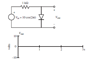
Sketch the output waveform for the circuit of Fig. 1 ΚΩ 10 cos 271 V Vou Vou 10 Vout o Vout Vin 035 075 1 1252 225 275 3s -10 Problem 2 Solve problem 1 using a real approximation of the diode. In contrast to the output waveform of the inverting amplifier circuit we note that the input and output are in phase for the noninverting amplifier.
Sketch the output waveform for the switch transistor circuit of figure 2. At which time it stays at the appropriate. Electronic Devices and Circuit Theory 11th.
Sketch the output waveform resulting in Fig. Draw the resulting output waveform for the circuit of Fig. The output waveform is sketched in Fig.
Explain the effect of a filter capacitor being. The diodes are arranged to cause clipping at the common node shared by D 1 D 2 R 1 and C 1 -- namely V a. The AC voltage source is texV_ocosomegattex with texV_otex 10V and texomegatex 2000radsec.
Sketching Op Amp Circuit Inputs and Outputs 1 Sketch V in. 67 along with the input waveform for comparison. Materials Devices and Simple Circuits.
V_o 47 volts V o. Sketch the output waveform for the circuit of Fig. Consider positive half cycle Diode will be reverse biased and acts as the open circuit shown below.
Sketch the output waveform resulting in Fig. About Press Copyright Contact us Creators Advertise Developers Terms Privacy Policy Safety How YouTube works Test new features Press Copyright Contact us Creators. Sketch the output waveform and the voltage transfer characteristic for the circuit of Figure P924.
In the first portion of the video we showed how to quickly draw output waveform for a very simple circuitIn the last portion of this video we draw output. Also give explanation of the waveform. An example is illustrated on the left hand side.
I need the answer at 20 minute. Sketch the output waveform resulting in. Sketch the output waveform of the circuit shown in figure below.
A Full Wave Rectifier is a circuit which converts an ac voltage into a pulsating dc voltage using both half cycles of the applied. Draw the resulting output waveform for the circuit of Fig. Draw a voltagetime diagram of the output waveform.
Sketch the output waveform for the circuit of Fig. Show a couple of cycles 2 Sketch output lightly with correct sign based on sign of gain. Now when the input voltage 20sinωt increase beyond 5V then path of diode 5V battery will offer very low resistance so the current passes through diode and battery and output across A and B remain 5V graph CD.
V o 1 2 7. I Sketch the output waveform from an AND gate for the inputs A and B shown in the figure. Sketch the output waveform resulting in Fig.
When the input voltage goes to -12 volts the normal diode turns off and the input voltage is in series with the voltage across the capacitor. VIN is the yellow waveform 10 Vp-p VOUT is the blue-green aqua waveform the red is VIN - VOUT but leave that aside. Draw the resulting output waveform for the circuit of Fig.
The circuit diagram and the associated waveforms are shown below. Figure 1 shows Series Negative Clipper with Positive Bias Voltage Connected in Series when Vin 0 diode will be forward bias till Vin reaches 1V output voltage will be 1V and when Vin 1V then Vo Vin 1 V as shown in Figure 2. In each case the input is a symmetrical square wave input signal of amplitude 12 VWith the aid of a circuit diagram explain the operation of a half-wave rectifier operating into a resistive load.
Note that it follows the input voltage until one or the other diode conducts. I have posted a diode circuit question in the attachment Ok I think it should be a sine curve with a 10 V amplitude but am not too sure about the period. The result is shown in Figure 1.
Sketch the output voltage as a function of time. Sketch the output waveform for the circuit of Fig. Terry Sturtevant Electronics Sketching Op Amp Circuit Inputs and Outputs.
Sketch the output waveform of the bartleby. Sketch the output waveform for each of the circuits shown in Fig. Ii If the output of the above AND gate is fed to a NOT gate name the gate of the combination so formed.
Solved Sketch The Output Waveform For Vout In The Following Circu Chegg Com

Draw The Output Waveform For The Circuit Shown Below

Print The Page And Draw The Output Waveform On This Grid Inductors 9v Battery Connector Flexible Wire


0 Comments